I'm not responsible for anything that happens because of your use of the information on this page. Use at your own risk. Though I've tried to make sure that the information here is accurate, I DO NOT guarantee that it is.
The 8500TVX is an old motherboard that was made by Biostar. It comes in several versions. Versions older than 2.3 can only run a Pentium MMX or Cyrix MII (M2) up to 166 MHz, but not up to their full speed. Versions 2.3 and newer of the board should be able to run these faster processors without modification. This does not apply to regular (classic) Pentium 200 processors, only to the MMX processors of 200 MHz and higher.
The clock multiplier is set on most CPUs by setting certain pins on the processor to "high" or "low". On Intel (and AMD I think), these are called BF0 and BF1 (BF = bus frequency) and on Cyrix, CLKMUL0 and CLKMUL1 (CLKMUL = clock multiplier). CPUs have a default multiplier so that, if none of the BF (a.k.a. CLKMUL) pins are set, they run at that frequency. This is set by internal resistors in the processor that either set the pins high (pull-up resistor) or low (pull-down resistor). The original Pentium had internal pull-up resistors on both BF0 and BF1. Since these are high by default, I guess Biostar saw no reason to provide a way to force them high, so the old versions of 8500TVX cannot set a pin high, they can only set it low or not set it at all (letting the high default take over).
The original default multiplier was 1.5x, indicated by both pins being high. On the new MMX processors, they needed another multiplier: 3.5x. So they reused the high-high setting for this. They then had to change the default to 2.0x, which is indicated by BF0 being set to 0 (0 = low) and BF1 being set to 1 (1 = high). This is why we have a problem. Since now BF0 is low by default and the 8500TVX only has the ability to pull it low (which it already is), we are left with no way to set BF0 to high. That makes it impossible to use a multiplier above 2.5x. Fortunately, that's not hard to fix...
Take a look at this chart. A number 1 means high and 0 means low.
| Multiplier | BF1 | BF0 |
|---|---|---|
| Pentium classic default (1.5x) | 1 | 1 |
| Pentium MMX default (2.0x) | 1 | 0 |
| 1.5x | 1 | 1 |
| 2.0x | 1 | 0 |
| 2.5x | 0 | 0 |
| 3.0x | 0 | 1 |
| 3.5x | 1 | 1 |
To use 3.0x and 3.5x, allowing 200-233 MHz, we need to set BF0 high. To do this we need to tie pin BF0 to the Vcc3 voltage pins through a resistor (I used a 1kΩ). This fix is easy and safe (if done carefully) because you won't need to do any soldering on the motherboard itself. You won't even need to take the motherboard out of the case. It can all be done using the jumpers on the board. You may also need a BIOS update, especially for Cyrix MII processors. See the BIOS update section.
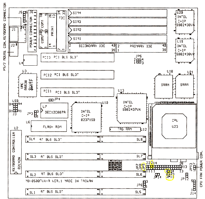
I highlighted the important jumpers on the diagram above (taken right off the Biostar web site). Since the Pentium MMX and Cyrix MII processors are dual-voltage, you should already have JP11 fully open. I found that the TOP 2 pins (numbered 2 and 4 in the diagram) are connected to the Vcc3 pins. I found that BF0 is linked to the TOP pin (number 2) of JP9 and BF1 is linked to the TOP pin (number 2) of JP8. The bottom (number 1) pins of JP8 and JP9 go directly to ground. So when you put a jumper on JP8 or JP9 what you are doing is tying BF1 or BF0 to ground (therefore setting it low). Anyway, what we need to do is to get a resistor in between the top pin (number 2) of JP9 and one of the top pins (number 2 or 4, I used number 2) of JP11. This will apply voltage to the BF0 pin, setting it high. You can do this any way you want, but if you don't have any ideas, you can try my method, which I'll describe now.
You need 2 spare little plastic jumpers, a tiny bit of wire (about gauge 24), and a resistor. I used a 1kΩ resistor. Don't use anything higher than 2k. Cut 2 small pieces of wire, about 1 inch long each and strip about 1 cm of insulation off of one end of each of them, and on the other end strip off however much you'll need to solder them to the resistor. Try to cut the 1 cm end just a little and on an angle so that it's kind of sharp. Get a needle nose pliers or something like that and push the wire down into one hole of a jumper from the top. (One side of the jumper is plastic with 2 holes in it and the other is a piece of metal with 2 holes in it. The top is the plastic side.)
The small metal piece inside the plastic case of the jumper might come out as you try to push the wire in. If that happens, it's okay. If the wire goes through fine for you, then you don't need to worry about this paragraph. If the metal piece comes out, get a pocket knife or something and try to widen one of the little clip-like things at the top side of the metal piece that fell out and then push the metal piece back into the plastic case only part way, so at least 1 mm of the bottom of the metal piece still is outside of the plastic case. Now slide the wire into the top of the jumper on the side with the clip that you widened and push it all the way through and out the hole in the bottom of the metal piece, then push the metal piece all the way back in.
Push one of the wires into each jumper in this way. There may be an easier way so you can play with it any way you want.
By now you should have 2 jumpers with pieces of wire going into the top of each one and coming out the bottom of the jumper a few millimeters. Bend the part that sticks out the bottom up around the side of the plastic case if you can. This will prevent the wire from slipping back out. If you can't bend it around, just clip any excess off and be careful when handling the jumper not to pull the wire out.
Now you just need to solder one of the wires coming from the jumpers to each end of the resistor. That's all you have to do. Now you should basically have 2 jumpers with a resistor between them. Plug the open hole of one of the jumpers onto pin 2 of JP11 and the other jumper to pin 2 of JP9.
Use the table below to help you set the jumpers for whatever multiplier you want. If you need to close JP8, just use a regular un-modified jumper like you would normally. To tie pin 2 of JP9 to pin 2 JP11 with the resistor, see the instructions above.
| Multiplier | JP8 | JP9 |
|---|---|---|
| 2.0x | open | closed |
| 2.5x | closed | closed |
| 3.0x | closed | tied to JP11 w/ resistor |
| 3.5x | open | tied to JP11 w/ resistor |
One of the resistor jumpers should be plugged onto pin 2, which is the TOP of JP9 NOT the bottom! Plug the other end onto one of the top pins, that is pin 2 or pin 4 (I haven't tested pin 4, so I recommend using pin 2) of JP11. BE CAREFUL. Get the right pins! Check and recheck, since getting the wrong pins or getting short circuits could toast the board and/or CPU!
Important: The Cyrix MII and Pentium MMX are dual-voltage processors. This is different from the original Pentium. Use the manual to find the right jumper settings for different CPU voltages. Also, some of these CPUs could potentially draw more power than the board was originally designed for. It feels like the Pentium MMX at 233 MHz is actually more efficient than some of the older processors because it is fairly cool to the touch even under load. However you still need to use caution not to overload the CPU voltage regulators. I do not remember for sure, but I think the Cyrix MII was drawing a lot of power. If the CPU voltage regulators overheat, damage will likely result to the regulators or other components, quite possibly including the CPU.
You may need a BIOS update for newer processors. If your processor seems unstable at these higher speeds, try increasing the core voltage by opening JP14.
I got information from these places:
Comments and questions are welcome. E-mail address: contact delete-this-before-sending _AT_ vobarian.com (Obviously, delete the extraneous words and replace _AT_ with @. This is to reduce spam.)
Mountains & clouds at top of page (clouds.jpg) taken from photo by Oswald Skene / DHD Multimedia Gallery
©2009 Chad Berchek - everything here unless otherwise noted

 Home
Home 8500TVX